
Description
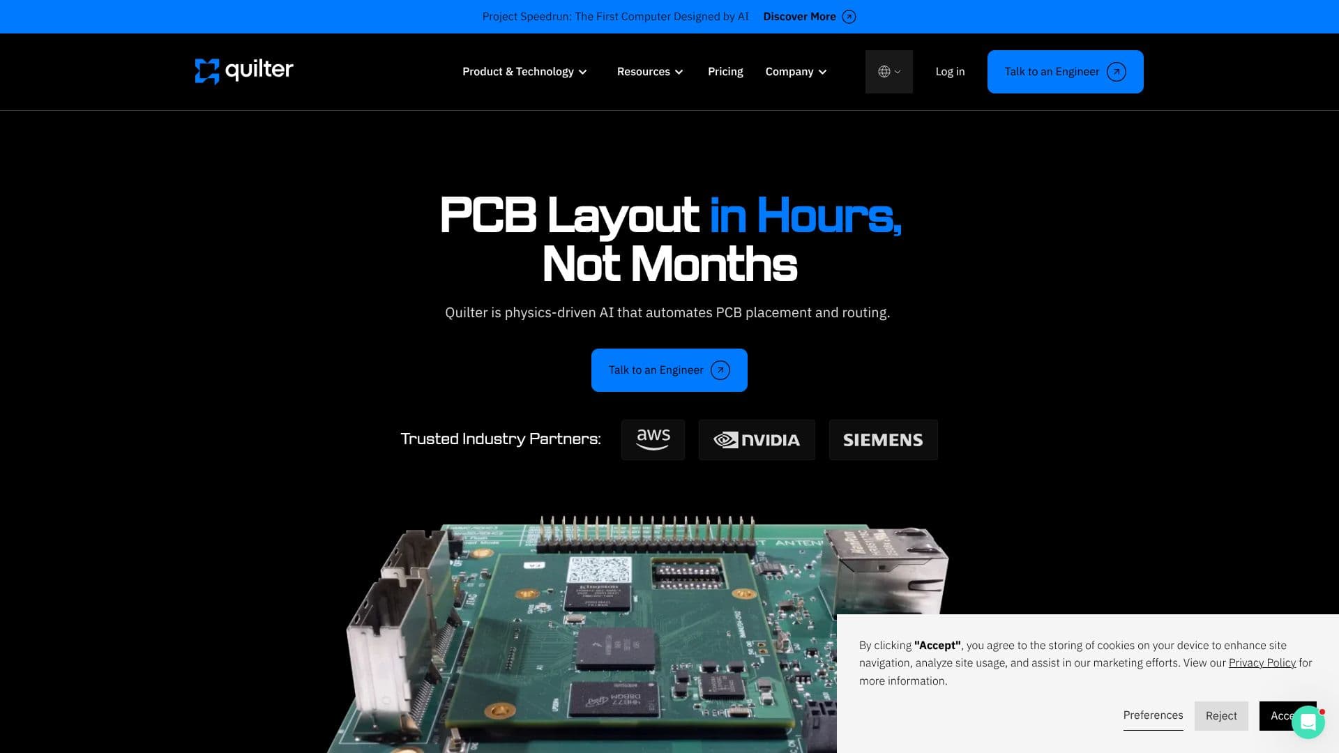
Quilter is an AI-powered platform designed to automate the critical and time-consuming process of PCB layout. By employing physics-driven reinforcement learning, Quilter actively explores thousands of potential board designs, validating every trace against physical constraints to ensure functionality. This approach significantly reduces the time from schematic to a fabrication-ready design, compressing cycles that traditionally take weeks into mere hours.
Read More
The platform is built to augment, not replace, the expertise of PCB designers and electrical engineers. It handles non-core layout tasks, freeing up valuable engineering bandwidth for more complex and innovative work. Quilter's workflow allows users to upload existing projects from Altium, Cadence, Siemens, or KiCAD, define board outlines, pre-place connectors, and set floorplans, maintaining user control over critical design parameters.
Quilter's physics-aware design capabilities mean it identifies and accounts for essential elements such as bypass capacitors, impedance-controlled nets, and differential pairs, presenting these for user review. This transparency ensures designers understand what the AI has addressed and what requires further attention. The ability to iterate rapidly is a core benefit, enabling users to test multiple stack-ups, manufacturers, and form factors in parallel, accelerating the design validation process.
For industries like semiconductors, robotics, consumer electronics, and aerospace & defense, Quilter offers substantial time savings. Semiconductor bring-up can be ready in a single workday, while robotics and consumer electronics boards can be fabricated-ready within hours. Aerospace and defense projects benefit from faster board bring-up for validation and TRR. The platform is also designed with robust IP protection and cybersecurity best practices, offering options for self-hosted deployments to maintain data control.
Quilter's value proposition lies in its ability to accelerate hardware development cycles, increase engineering productivity, and enable faster innovation. By automating routine layout tasks and providing physics-validated design candidates, it empowers teams to out-innovate competitors and bring complex electronic products to market more efficiently. The tool is continuously improving, with ongoing development in areas like blind & buried vias, length matching, and RF pre-routing.
- CategoryRobotics & AI Hardware
- Pricing ModelContact for Pricing
- DeploymentSelf-Hosted Available
- PlatformsWeb
Quilter's Core Features
Physics-driven AI for PCB layout automation
Generates multiple design candidates in hours
Physics validation for every trace
Integrates with Altium, Cadence, Siemens, and KiCAD
Automates PCB placement and routing
Identifies critical design elements like bypass capacitors and impedance-controlled nets
Enables rapid iteration with multiple stack-ups and form factors
Provides transparent design review with clear feedback
Seamless board handoff in original submission format
Reinforcement learning for active design exploration
No training on user data; learns from synthetic boards and physics
Self-hosted deployment option available
Data encrypted at rest and in transit
Enterprise-grade support for mission-critical environments
How to use Quilter?
Configure: Upload your schematic and define board outline, pre-place connectors, and floorplan.
Control: Specify design constraints and parameters for the AI.
Generate: Let Quilter's physics-driven AI explore thousands of layout candidates.
Review: Examine physics-validated designs and identify areas for further refinement.
Iterate: Test multiple stack-ups, manufacturers, or form factors in parallel.
Handoff: Receive fabrication-ready files in your original CAD format for final checks and manufacturing.
Quilter's Use Cases
- Automated PCB Layout
- Design Iteration
- Board Bring-up Acceleration
- IC Evaluation Boards
- Test Fixtures & Harnesses
- Design Validation Boards
- Backplane & Interconnect Boards
- Semiconductor Design
- Robotics Design
- Consumer Electronics